domingo, 29 de enero de 2012

Cooling Effects of Graphene May Lead to Longer-Lasting Computers and Cellphones


A novel research conducted by scientists at UT Dallas paves the way to develop high-efficiency cooling solutions for producing quieter electronics with improved operating life.


"A laptop fan pumps heat out of the system, but heat removal starts with a chip on the inside. Engineered graphene could be used to remove heat – fast.”


According to Dr. Kyeongjae “KJ” Cho from UT Dallas, heat removal begins within a chip and engineered graphene can be utilized to eliminate heat rapidly. Cho is investigating the thermal conductivity of the wonder material, graphene. A paper reported in the Nature Materials journal is in line with Cho’s statement. The paper demonstrates that graphene is capable of conducting heat at a rate 20 folds quicker than that of silicon, a commonly used semiconductor material in electronics.

For the Nature Materials paper, UT Austin’s research team carried out a study on heat transfer characteristics of graphene. The team heated the center of a portion of the material using a laser beam. It then measured the difference in temperature between the middle and the edge of the material. Cho’s theory assisted the team to demonstrate its findings.

Cho stated that the performance of an electronic device gets affected as it heats up. Hence the efficiency and operating life of an electronic device improves proportionately with the rate of removal of heat, Cho added.

Cho further said knowledge of the heat transfer mechanism of a two-dimensional graphene system will help the researchers to manipulate the material’s use in day-to-day semiconductor devices. To achieve this, Cho together with Hengji Zhang from UT Dallas is working on a follow-up article that describes the way of controlling graphene’s thermal conductivity.

Click here for the complete article.

martes, 24 de enero de 2012

Nanobots para contra el cáncer(de nuevo)


Tal como ya hemos escuchado muchas veces en programas sensacionalistas de televisoras semicientificas internacionales, la nanotencologia puede ser implementada en si para tratar enfermedades complicadas como el mimo cancer.
Investigadores del Wyss Institute for Biologically Inspired Engineering de Harvard han creado robots a partir del ADN . Estos robots hechos en nano escala  podrían ser usados para dar instrucciones directamente a las células del paciente. Con esta técnica se podrían combatir diferentes enfermedades y hacer que las células cancerígenas se maten a sí mismas. Los robotcitos están construidos usando la técnica del Origami de ADN (leer abajo).
En este caso, el ADN fue diseñado para operar en un simple sistema de lógica, como una computadora. Tiene la forma de un barril, con dos partes del mismo separadas por una bisagra. Diferentes químicos se pueden introducir dentro del robot. Luego, cuando encuentra la molécula particular por la que fue diseñada –como una proteína que solo se encuentra en una célula cancerígena- activa un switch que abre el barril y libera el químico que lleva dentro.
El Dr. Ido Bachalet dijo en un comunicado de prensa  “Se puede pensar en una clase de combinación de apertura, solo cuando ambos marcadores coinciden en el lugar, se puede abrir la puerta del robot.”
Estos Robots son ideales para suministrar químicos dentro del cuerpo, es compatible con el sistema biológico y es naturalmente biodegradable debido a su emsamblaje con base en adn. Además, debido  a que los robots pueden actuar solamente sobre ciertas células, es posible usar dosis menores de medicamentos, lo que limitaría el efecto tóxico y sería más efectivo.  Aún está en “Beta Test”, con puras cajas de Petri, pero sus promesas son importantes.

fuente total: sciencemag.org/content/335/6070/831.abstract

domingo, 22 de enero de 2012

Study Reveals Molecular Self-Assembly Process Follows Different Pathways

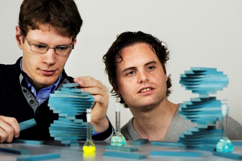
Researchers at Eindhoven University of Technology (TU/e) have succeeded in monitoring and controlling a molecular self-assembly process via different pathways. While it was formerly thought that the molecules form the right structure by themselves, this research shows that the assembly process can follow different pathways yielding different structures; in this case polymer chains with left- and right-handed helical directions. This new knowledge is of great importance for the understanding of supramolecular polymers, in which small differences in the way the molecular building blocks are organized can have a large influence on the properties of the resulting material.

Molecular building blocks form a supramolecular structure by arranging themselves through the molecular self-assembly process. Manipulating the molecular self-assembly process principles leads to the development of novel materials with innovative properties, for instance, a self-repairing coating. Since the way of self-assembly of the building blocks plays a major role in the properties of the resulting materials, a slight difference in their assembly can result in materials with unique properties.

In the experiment, the research team studied a molecular building block called S-chiral oligo (p-phenylenevinylene) or SOPV utilizing pectroscopy. SOPV initially self-assembled into unstructured clusters and then into well-arranged left-handed helical structures look like a spiral staircase. Earlier, it was believed that a molecule can self-assemble only into a single end-product and the process’ intermediate steps are not significant and cannot be studied due to their rapid occurrence.

According to the TU/e research team, intermediate process steps are highly significant, as they guide to different variants. For instance, rapid occurrence of SOPV’s self-assembly process produces spiral staircase structures featuring an opposite helical direction. However, when tartaric acid is added temporarily to the SOPV molecules, the assembly process is forced totally towards this alternative structure. In-depth analysis demonstrates that these two helical forms battle for the available molecular building blocks.

The article Pathway Complexity in Supramolecular Polymerization was published online on January 18, 2012 on the Nature website, and will also appear in the printed edition in the near future. The authors are Peter Korevaar, Subi George, Bart Markvoort, Maarten Smulders, Peter Hilbers, Albert Schenning, Tom de Greef and Bert Meijer, all at Eindhoven University of Technology. The DOI number is 10.1038/nature10720.

Source.

miércoles, 18 de enero de 2012

Stop SOPA


A protein transistor made of an antibody molecule


A major challenge in molecular electronics is to attach electrodes to single molecules in a reproducible manner to make molecular junctions that can be operated as transistors. Several attempts have been made to attach electrodes to proteins, but these devices have been unstable. Here, we show that self-assembly can be used to fabricate, in a highly reproducible manner, molecular junctions in which an antibody molecule (immunoglobulin G) binds to two gold nanoparticles, which in turn are connected to source and drain electrodes. We also demonstrate effective gating of the devices with an applied voltage, and show that the charge transport characteristics of these protein transistors are caused by conformational changes in the antibody. However, because of limitations in current technology, the achievement of these goals is very challeng- ing. Although, some isolated examples of such devices and architectures have been demonstrated, they exhibit only moderate or limited performance, or are constructed via sophisticated multistep methodologies. In this publication Mentovich and his team suggest and demonstrate a universal method in which a new type of nanometer-sized, ambipolar, vertical molecular transistor is fabricated in parallel fashion. This centralgate molecular vertical transistor (C-Gate MolVeT) is fabricated by a combination of conventional microlithography techniques and self-assembly methods. The general fabrication methodology of the C-Gate MolVeT allows the process to be adapted for various materials and systems.In this design, the nanometer channel length is determined by a protein-based self-assembled monolayer composed of bovine serum albumin protein, that is sandwiched between source and drain electrodes inside a microcavity, while a centered oxidized-metal-electrode column inside the cavity serves as the gate electrode. The results showed a transistor fully operational, that can be made with lithography thechniques, they messured the gate effect, and demonstrated the characteristic transistor curves when variating the voltage in the drain terminal.


The full article can be found in nanoletters:

A protein transistor made of an antibody molecule and two gold nanoparticles


lunes, 16 de enero de 2012

The Shear Flow Processing of Controlled DNA Tethering and Stretching for Organic Molecular Electronics.

The field of molecular electronics explores molecular building blocks for the fabrication of ever-shrinking electronic elements. Much of the excitement of this area has arisen from the huge prospect of size reduction in electronics offered by the molecular level control of their properties. However, one of the biggest obstacles for molecular electronic to be practically exploited is the lack of techniques to make reliable and reproducible electrical contacts to single organic molecules of interest.

Scientists at Stanford University address this challenge by exploiting DNA, one of the most versatile and powerful molecules available for molecular fabrication and self/assembly, as a molecular template for metal electrodes. DNA molecules can be chemically linked to a variety of single organic molecules and can also be used as a template for metallic nanostructures.

The authors have developed a reproducible surface chemistry for tethering DNA molecules at tunable density and demonstrated shear flow processing as a rationally controlled approach for stretching/aligning DNA molecules of various lengths.

The proposed strategy starts with the synthesis of hybrid DNA – organic molecule – DNA (DOD) structures, followed by subsequent stretching/alignment and double tethering of the DOD assemblies between two microscopic metal electrodes. Further metallization of the DNA segments completes the fabrication of metal electrode – organic molecule – metal electrode (M – O – M) structures, thus realizing the conducting contacts to organic molecules.

This approach that utilizes DNA as a templated bridge to connect single organic molecules and microscopic electrodes is a bottom-up approach to integration at the nanoscale. It represents an important step toward the building of increasingly complex molecular circuits.

Follow the link for the complete article.

The Shear Flow Processing of Controlled DNA Tethering and Stretching for Organic Molecular Electronics

Guihua Yu, Amit Kushwaha, Jungkyu K. Lee, Eric S. G. Shaqfeh, and Zhenan Bao

ACS Nano 2011 5 (1), 275-282

viernes, 13 de enero de 2012

Mauricio Terrones nombrado fellow de la AAAS

Mauricio Terrones, Profesor del Departament of Physics and Materials Science and Engineering en Penn State, ha sido nombrado Fellow of the American Association for the Advancement of Science 2011. Este año, 539 nuevos miembros fueron seleccionados y recibirán su reconocimiento el 18 de Febrero de 2012 durante el Congreso de la AAAS (American Associaton for the Advance of Science) en Vancouver, British Columbia. Para ver los nombres de todos los premiados, pueden ver esta [ LIGA ].


Felicidades Mauricio.

NanoGold-Ears

les dejo el link para que lo revisen :)

Se trata del micrófono más pequeño que se ha podido crear, tan sensible que se planea detectar decibeles a un nivel inferior a la de cualquier ser vivo; incluso para poder escuchar lo que dicen las células y virus :O

martes, 10 de enero de 2012

Simposio de Nanociencias y Nanomateriales, Ensenada


El Centro de Nanociencias y Nanotecnología (CNyN) de la UNAM en Ensenada, BC, está organizando el Primer Simposio Internacional en Nanociencias y Nanomateriales para conmemorar 30 años de actividades de investigación científica en Ensenada. Entre los destacados invitados a este evento se encuentran:


  • Miquel Salmerón (UC Berkeley)

  • Joe Greene (University of Illinois)

  • Gleb Finkelstein (Duke University)

  • Rodolfo Zanella (CCADET-UNAM)

  • Sergio Ulloa (Ohio University)

  • Neha Singh (J. A. Wollam, Inc)

  • Juan Muñoz (CINVESTAV-Querétaro)

  • Joanna McKittrick (UCSD)

  • Valery Fokin (Scripps Research Institute)

  • Ana Cremades (Universidad Complutense de Madrid)

  • Darío Bueno-Baqués (CIQA)

  • Francisco Zaera (UC Riverside)

  • Leonel Cota (CNyN-UNAM)

El evento no tiene costo (excepto los Talleres avanzados en "Técnicas de Vacío", "Microscopía" y "Espectroscopía de Superficies" que tienen una cuota de $200.00 pesos) y tendrá por sede el Hotel Cortez en Ensenada. Hay espacio para presentaciones de trabajos (orales o carteles) con fecha límite el 20 de Enero. ¡No falten!

Mas información en: