Mostrando las entradas con la etiqueta NT440. Mostrar todas las entradas

domingo, 29 de abril de 2012

USC Researchers Develop Path to Liquid Solar Cells

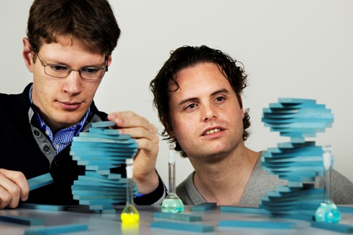
A USC scientist treats a glass slide with nanocrystals. (Photo/Dietmar Quistorf)

Scientists at USC have developed a potential pathway to cheap, stable solar cells made from nanocrystals so small they can exist as a liquid ink and be painted or printed onto clear surfaces.
The solar nanocrystals are about four nanometers in size – meaning one could fit more than 250 billion on the head of a pin – and float them in a liquid solution, so “like you print a newspaper, you can print solar cells,” said Richard L. Brutchey, assistant professor of chemistry at the USC Dornsife College of Letters, Arts and Sciences.
Brutchey and USC postdoctoral researcher David H. Webber developed a new surface coating for the nanocrystals, which are made of the semiconductor cadmium selenide. Their research is featured as a “hot article” in Dalton Transactions, an international journal for inorganic chemistry.
Liquid nanocrystal solar cells are cheaper to fabricate than available single-crystal silicon wafer solar cells but are not nearly as efficient at converting sunlight to electricity. Brutchey and Webber solved one of the key problems of liquid solar cells: how to create a stable liquid that also conducts electricity.
In the past, organic ligand molecules were attached to the nanocrystals to keep them stable and to prevent them from sticking together. These molecules also insulated the crystals, making the whole thing terrible at conducting electricity.
“That has been a real challenge in this field,” Brutchey said.
Brutchey and Webber discovered a synthetic ligand that not only works well at stabilizing nanocrystals but actually builds tiny bridges connecting the nanocrystals to help transmit current.
With a relatively low-temperature process, the researchers’ method also allows for the possibility that solar cells can be printed onto plastic instead of glass without any issues with melting, resulting in a flexible solar panel that can be shaped to fit anywhere.
As they continue their research, Brutchey said he plans to work on nanocrystals built from materials other than cadmium, which is restricted in commercial applications due to toxicity.
“While the commercialization of this technology is still years away, we see a clear path forward toward integrating this into the next generation of solar cell technologies,” Brutchey said.
The National Science Foundation and USC Dornsife funded the research.


Follow this link for more information.

New Faster and More-Efficient Technique to Generate Single Photons


Georgia Tech graduate student Yaroslav Dudin and professor Alex Kuzmich (l-r) adjust optics as part of research into the production of single photons for use in optical quantum information processing and the study of certain physical systems

Georgia Tech professor Alex Kuzmich and graduate student Yaroslav Dudin have devised a new faster and more-efficient technique based on a phenomenon called Rydberg blockade to generate single photons that can be utilized to explore the disorder and dynamics in specific physical systems and in optical quantum information processing.
Kuzmich and Dudin have been working on quantum information systems that are based on mapping of atomic information onto confined photon pairs. They used Raman scattering technique for this research. However, this technique was inefficient to generate the required number of confined photons for complex systems. To overcome this issue, they have developed the new technique.
The new technique leverages the novel properties of atoms, which have one or more electrons in the Rydberg state. These highly excited atoms have a principal quantum number over 70, demonstrate powerful electromagnetic properties, and interplay strongly with each other. These properties of a Rydberg atom prevent the generation of additional Rydberg atoms within a region of 10-20 µm due to the Rydberg blockade phenomenon. This single Rydberg atom is then transformed to a photon, thus ensuring the generation of one photon from a rubidium ensemble comprising numerous densely-packed atoms.
The researchers produced the Rydberg atom by irradiating a cloud of hundreds of laser-cooled rubidium 87 atoms entangled in an optical lattice, using lasers. The irradiation excited a single atom from the whole ensemble into the Rydberg state. At this state, the Rydberg blockade phenomenon prevents the generation of additional Rydberg atoms by modifying the atomic level energies, thus producing only one Rydberg atom. Since Rydberg atoms demonstrate strong interaction within an area of 10-20 µm, the researchers restricted the volume of their cloud of rubidium atoms, thus ensuring the formation only one Rydberg atom from the ensemble.
Using an additional laser field, the researchers then converted this Rydberg atom into a quantum light field with the same statistical properties of the Rydberg atom. Dudin informed that this new photon source is thousand folds quicker than current systems. The researchers used Rydberg atoms that have a principal quantum number of roughly 100. The next step is to develop a quantum gate in between light fields.


Strongly Interacting Rydberg Excitations of a Cold Atomic Gas. Y. O. Dudin and A. Kuzmich. Science 1217901Published online 19 April 2012 [DOI:10.1126/science.1217901]


Follow this link for more information.

DNA Origami Nanoplate Serves as Smart Lid for Solid-State Nanopore Sensor


This illustration shows how a DNA origami nanoplate with a central aperture can serve as a smart lid or "gatekeeper" for a solid-state nanopore sensor. Researchers at the Technische Universitaet Muenchen have demonstrated that this arrangement can be used to filter biomolecules by size or to "fish" for specific target molecules by placing single-strand DNA receptors inside the aperture as "bait." With further research, they suggest, it might be possible to use such single-molecule sensors as the basis of a novel DNA sequencing system.


Technische Universitaet Muenchen (TUM) researchers have used DNA origami to improve the capabilities of solid-state nanopores. They have combined new capabilities for sensing of single-molecules.
The researchers fitted nanoscale DNA-based nanoscale cover plates on to solid-state nanopores. On these plates, DNA origami was used to form central apertures designed for different "gatekeeper" functions.
Bionanotechnology has enabled single-molecule sensitivity for performing label-free protein screening. Researchers belonging to Prof. Hendrik Dietz's group have been improving control over techniques used for DNA origami, while researchers belonging to Dr. Ulrich Rant's group have been investigating the techniques for solid-state nanopore sensors, wherein a biomolecule is made to pass through a hole, which is of nanometer scale in a thin semiconductor slab. The research groups are collaborating for this study.
The concept involves placing a DNA origami "nanoplate" on top of a solid-state nanopore with a conical taper. The plate is placed over the narrow end of the taper. Controlling the aperture size will enable filtration of the desired size of molecules. Single-stranded DNA receptors are placed in the aperture to act as “bait” and this will enable the detection of "prey" molecules in a sequence-specific manner. This can lead to applications for detecting and screening DNA sequences.
The researchers confirmed the self-assembling ability of specially designed DNA origami nanoplates and their placement on solid-state nanopores. Bait/prey detection of particular target molecules and biomolecule size-based filtering were demonstrated.
The ability of DNA origami gatekeepers to allow the passage of small ions may also be an unwanted leakage current in certain applications. DNA sequencing and other applications may have to face such hurdles.


DNA Origami Gatekeepers for Solid-State Nanopores Ruoshan Wei, Thomas G. Martin, Ulrich Rant, and Hendrik Dietz Angewandte Chemie International Edition on-line, April 4, 2012. DOI: 10.1002/anie.201200688


Follow this link for more information.

NIST Study Proves Thermal Stability of Nanometer-Thick Films for Organic Electronics


A research team from the National Institute of Standards and Technology (NIST) has helped an international research team to verify the stability of an ultrathin membrane using near-edge X-ray absorption fine-structure spectroscopy (NEXAFS).
The ultrathin membrane developed by the international research team can be used as a key component for a new class of flexible, sterilizable organic electronics for use in medical applications. The team is headed by scientists from the University of Tokyo, with members from the Princeton University, Hiroshima University, the Japan Science and Technology Agency, the Max Planck Institute for Solid State Research and Nippon Kayaku, a Tokyo-based company.
The international research team has developed an innovative gate material that enables high-temperature sterilization of organic transistors, thus making them suitable for medical applications such as soft pacemakers and implantable devices. This gate material assembles itself into an ultrathin single layer of tightly packed linear molecules that assemble at a small angle to the surface. The team informed that this self-assembled monolayer (SAM)’s thickness can be down to 2 nm.
Structural measurements of SAM were performed at the NIST low-energy X-ray beam line located at the National Synchrotron Light Source in New York. Samples of the ultrathin film from prior and after heat treatment were tested on the NIST beamline utilizing NEXAFS technique to measure the thermal stability and molecular orientation of the film.
The NEXAFS technique is capable of detecting chemical bonds at the surface and in the interior of the sample. For example, it can show the disparity between a single carbon bond and a double carbon bond within a molecule. The NEXAFS measurements proved that the SAM ultrathin films were able to maintain their integrity and stability even at temperatures above 150°C.

K. Kuribara, H. Wang, N. Uchiyama, K. Fukuda, T. Yokota, U. Zschieschang, C. Jaye, D. Fischer, H. Klauk, T. Yamamoto, K. Takimiya, M. Ikeda, H. Kuwabara, T. Sekitani, Y-L. Loo and T. Someya. Organic transistors with high thermal stability for medical applicationsNature Communications. 3, 723. Mar. 6, 2012. doi:10.1038/ncomms1721

Follow this link for more information.

miércoles, 7 de marzo de 2012

The smallest conceivable switch

For a long time miniaturization has been the magic word in electronics. Dr. Willi Auwaerter and Professor Johannes Barth, together with their team of physicists at the Technische Universitaet Muenchen (TUM), have now presented a novel molecular switch in the journal “Nature Nanotechnology.” Decisive for the functionality of the switch is the position of a single proton in a porphyrin ring with an inside diameter of less than half a nanometer. The physicists can set four distinct states on demand.


Porphyins are ring-shaped molecules that can flexibly change their structure, making them useful for a wide array of applications. Tetraphenylporphyrin is no exception: It likes to take on a saddle shape and is not limited in its functionality when it is anchored to a metal surface. The molecule holds has a pair of hydrogen atoms that can change their positions between two configurations each. At room temperature this process takes place continuously at an extremely rapid rate.

In their experiment, the scientists suppressed this spontaneous movement by cooling the sample. This allowed them to induce and observe the entire process in a single molecule using a scanning tunneling microscope. This kind of microscope is particularly well suited for the task since – in contrast to other methods – it can be used not only to determine the initial and final states, but also allows the physicists to control the hydrogen atoms directly. In a further step they removed one of the two protons from the inside of the porphyrin ring. The remaining proton could now take on any one of four positions. A tiny current that flows through the fine tip of the microscope stimulates the proton transfer, setting a specific configuration in the process.

Although the respective positions of the hydrogen atoms influence neither the basic structure of the molecule nor its bond to the metallic surface, the states are not identical. This small but significant difference, taken together with the fact that the process can be arbitrarily repeated, forms the basis of a switch whose state can be changed up to 500 times per second. A single tunneled electron initiates the proton transfer.

The molecular switch has a surface area of only one square nanometer, making it the smallest switch implemented to date. The physicists are thrilled by their demonstration and are also very happy about new insights into the mechanism behind the proton transfer resulting from their study. Knud Seufert played a key role with his experiments: “To operate a four-state switch by moving a single proton within a molecule is really fascinating and represents a true step forward in nano-scale technologies.”

This research was funded by the European Research Council (ERC Advanced Grant MolArt, No. 247299), the Excellence Cluster Munich-Centre for Advanced Photonics (MAP) and the Institute for Advanced Study of the TU Muenchen.

Original publication:


Auwärter, Willi, Knud Seufert, Felix Bischoff, David Ecija, Saranyan Vijayaraghavan, Sushobhan Joshi, Florian Klappenberger, Niveditha Samudrala, and Johannes V. Barth. "A surface-anchored molecular four-level conductance switch based on single proton transfer." Nature Nanotechnology 7: 41-46.

Click here for more information.


domingo, 19 de febrero de 2012

Konica Minolta Unveils Inkjet Printhead for Printed Electronics Applications


Tokyo (February 14, 2012) - Konica Minolta IJ Technologies, Inc. (Konica Minolta) is pleased to announce that it has successfully developed a high-accuracy inkjet head capable of 1-picoliter drop size, the first for printed electronics applications by utilizing Konica Minolta's proprietary MEMS technologies for the first time. Sale of the new inkjet printhead in sample quantities is expected to start this spring.
The newly developed inkjet printhead “KM128SNG-MB” is a next-generation inkjet printhead manufactured with silicon MEMS technologies that utilizes semiconductor process technologies. Through MEMS technologies, Konica Minolta succeeded in developing highly accurate printhead construction (38mm width, in one row, 128 nozzles) capable of discharging in micro drop size. The company's proprietary technologies in ink flow path design and high-precision assembly processes have achieved layout of tiny-size droplet highly precisely and stably. Furthermore, the new inkjet printhead is highly resistant to various inks required for industrial applications and suitable to use with low-viscosity inks. Utilization of MEMS technologies has helped integration of nozzles and resulted in benefits such as compact inkjet printhead. In line with requests from the market in the future, further integration of nozzles will be an area of enhancement for time to come. Specific applications for the newly developed inkjet printhead will include, among others, OLED (Organic Light Emitting Diode) display patterning, OLED lighting thin-layer coating, and new manufacturing technologies for high-value-added displays for smartphones and similar devices that require high accuracy.
Printed electronics market, including next-generation flexible displays, is expected to grow to approximately two-trillion yen in 2020 (research by Konica Minolta), where utilization of the newly developed inkjet printhead is highly expected. Konica Minolta is a founding member of Japan Advanced Printed Electronics Technology Research Association (JAPERA) that was formed in 2011. Through its innovative inkjet technologies for industrial use, Konica Minolta has been contributing to the research and development activities for next-generation printed electronics technologies with even more energy-saving, resource-saving and highly productive features in the near future.

Major Applications
OLED display patterning, OLED lighting thin-layer coating, new manufacturing technologies for high-accuracy, high-value-added displays for smartphones and similar devices.

Click here or here for more information.

lunes, 13 de febrero de 2012

Sub-10nm Carbon Nanotube Transistor


Scientists at IBM T. J. Watson Research Center demonstrated the first sub-10nm CNT transistor, which is shown to outperform the best competing silicon devices with more than four times the diameter-normalized current density (2.14 mA/μm) at a low operating voltage of 0.5V. 
"We've made nanotube transistors at aggressively scaled dimensions, and shown they are tremendously better than the best silicon devices" said Aaron Franklin, main author of the paper.
To test how the size of a nanotube transistor affected its performance, Franklin's group made multiple transistors of different sizes along a single nanotube. This enabled them to control for any variations that might occur from nanotube to nanotube. First, they had to lay down a very thin layer of insulating material for the nanotube to sit on. And they developed a two-step process for adding electrical gates to the nanotube without damaging it. These techniques are by no means ready for manufacturing, but they enabled the IBM group to make the first nanotube devices smaller than 10 nanometers to test in the lab. The work is described online in the journal Nano Letters. 
Several major engineering problems remain, says Franklin. First, researchers have to come up with better methods for making pure batches of semiconducting nanotubes—metallic tubes in the mix will short out integrated circuits. Second, they must come up with a way to place large numbers of nanotubes on a surface with perfect alignment.
The superior low-voltage performance of this CNT transistor proves the viability of nanotubes for consideration in future aggressively scaled transistor technologies.

Sub-10 nm Carbon Nanotube Transistor

Aaron D. Franklin, Mathieu Luisier, Shu-Jen Han, George Tulevski, Chris M. Breslin, Lynne Gignac, Mark S. Lundstrom, and Wilfried Haensch
Nano Letters 2012 12 (2), 758-762

domingo, 29 de enero de 2012

Cooling Effects of Graphene May Lead to Longer-Lasting Computers and Cellphones


A novel research conducted by scientists at UT Dallas paves the way to develop high-efficiency cooling solutions for producing quieter electronics with improved operating life.


"A laptop fan pumps heat out of the system, but heat removal starts with a chip on the inside. Engineered graphene could be used to remove heat – fast.”


According to Dr. Kyeongjae “KJ” Cho from UT Dallas, heat removal begins within a chip and engineered graphene can be utilized to eliminate heat rapidly. Cho is investigating the thermal conductivity of the wonder material, graphene. A paper reported in the Nature Materials journal is in line with Cho’s statement. The paper demonstrates that graphene is capable of conducting heat at a rate 20 folds quicker than that of silicon, a commonly used semiconductor material in electronics.

For the Nature Materials paper, UT Austin’s research team carried out a study on heat transfer characteristics of graphene. The team heated the center of a portion of the material using a laser beam. It then measured the difference in temperature between the middle and the edge of the material. Cho’s theory assisted the team to demonstrate its findings.

Cho stated that the performance of an electronic device gets affected as it heats up. Hence the efficiency and operating life of an electronic device improves proportionately with the rate of removal of heat, Cho added.

Cho further said knowledge of the heat transfer mechanism of a two-dimensional graphene system will help the researchers to manipulate the material’s use in day-to-day semiconductor devices. To achieve this, Cho together with Hengji Zhang from UT Dallas is working on a follow-up article that describes the way of controlling graphene’s thermal conductivity.

Click here for the complete article.

domingo, 22 de enero de 2012

Study Reveals Molecular Self-Assembly Process Follows Different Pathways

Researchers at Eindhoven University of Technology (TU/e) have succeeded in monitoring and controlling a molecular self-assembly process via different pathways. While it was formerly thought that the molecules form the right structure by themselves, this research shows that the assembly process can follow different pathways yielding different structures; in this case polymer chains with left- and right-handed helical directions. This new knowledge is of great importance for the understanding of supramolecular polymers, in which small differences in the way the molecular building blocks are organized can have a large influence on the properties of the resulting material.

Molecular building blocks form a supramolecular structure by arranging themselves through the molecular self-assembly process. Manipulating the molecular self-assembly process principles leads to the development of novel materials with innovative properties, for instance, a self-repairing coating. Since the way of self-assembly of the building blocks plays a major role in the properties of the resulting materials, a slight difference in their assembly can result in materials with unique properties.

In the experiment, the research team studied a molecular building block called S-chiral oligo (p-phenylenevinylene) or SOPV utilizing pectroscopy. SOPV initially self-assembled into unstructured clusters and then into well-arranged left-handed helical structures look like a spiral staircase. Earlier, it was believed that a molecule can self-assemble only into a single end-product and the process’ intermediate steps are not significant and cannot be studied due to their rapid occurrence.

According to the TU/e research team, intermediate process steps are highly significant, as they guide to different variants. For instance, rapid occurrence of SOPV’s self-assembly process produces spiral staircase structures featuring an opposite helical direction. However, when tartaric acid is added temporarily to the SOPV molecules, the assembly process is forced totally towards this alternative structure. In-depth analysis demonstrates that these two helical forms battle for the available molecular building blocks.

The article Pathway Complexity in Supramolecular Polymerization was published online on January 18, 2012 on the Nature website, and will also appear in the printed edition in the near future. The authors are Peter Korevaar, Subi George, Bart Markvoort, Maarten Smulders, Peter Hilbers, Albert Schenning, Tom de Greef and Bert Meijer, all at Eindhoven University of Technology. The DOI number is 10.1038/nature10720.

Source.

lunes, 16 de enero de 2012

The Shear Flow Processing of Controlled DNA Tethering and Stretching for Organic Molecular Electronics.

The field of molecular electronics explores molecular building blocks for the fabrication of ever-shrinking electronic elements. Much of the excitement of this area has arisen from the huge prospect of size reduction in electronics offered by the molecular level control of their properties. However, one of the biggest obstacles for molecular electronic to be practically exploited is the lack of techniques to make reliable and reproducible electrical contacts to single organic molecules of interest.

Scientists at Stanford University address this challenge by exploiting DNA, one of the most versatile and powerful molecules available for molecular fabrication and self/assembly, as a molecular template for metal electrodes. DNA molecules can be chemically linked to a variety of single organic molecules and can also be used as a template for metallic nanostructures.

The authors have developed a reproducible surface chemistry for tethering DNA molecules at tunable density and demonstrated shear flow processing as a rationally controlled approach for stretching/aligning DNA molecules of various lengths.

The proposed strategy starts with the synthesis of hybrid DNA – organic molecule – DNA (DOD) structures, followed by subsequent stretching/alignment and double tethering of the DOD assemblies between two microscopic metal electrodes. Further metallization of the DNA segments completes the fabrication of metal electrode – organic molecule – metal electrode (M – O – M) structures, thus realizing the conducting contacts to organic molecules.

This approach that utilizes DNA as a templated bridge to connect single organic molecules and microscopic electrodes is a bottom-up approach to integration at the nanoscale. It represents an important step toward the building of increasingly complex molecular circuits.

Follow the link for the complete article.

The Shear Flow Processing of Controlled DNA Tethering and Stretching for Organic Molecular Electronics

Guihua Yu, Amit Kushwaha, Jungkyu K. Lee, Eric S. G. Shaqfeh, and Zhenan Bao

ACS Nano 2011 5 (1), 275-282