Mostrando las entradas con la etiqueta intronano o2012 146631. Mostrar todas las entradas

viernes, 30 de noviembre de 2012

Researchers Use Gold Nanoparticles for Low-Cost Semiconductors Production


A completely new method of manufacturing the smallest structures in electronics could make their manufacture thousands of times quicker, allowing for cheaper semiconductors. The findings have been published in the latest issue of Nature.
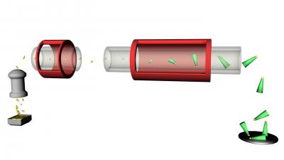

A completely new method of manufacturing the smallest structures in electronics could make their manufacture thousands of times quicker, allowing for cheaper semiconductors. (Credit: Lund University, Sweden)

Instead of starting from a silicon wafer or other substrate, as is usual today, researchers have made it possible for the structures to grow from freely suspended nanoparticles of gold in a flowing gas.
Behind the discovery is Lars Samuelson, Professor of Semiconductor Physics at Lund University, Sweden, and head of the University's Nanometre Structure Consortium. He believes the technology will be ready for commercialisation in two to four years' time. A prototype for solar cells is expected to be completed in two years.
"When I first suggested the idea of getting rid of the substrate, people around me said 'you're out of your mind, Lars; that would never work'. When we tested the principle in one of our converted ovens at 400°C, the results were better than we could have dreamt of", he says.
"The basic idea was to let nanoparticles of gold serve as a substrate from which the semiconductors grow. This means that the accepted concepts really were turned upside down!"
Since then, the technology has been refined, patents have been obtained and further studies have been conducted. In the article in Nature, the researchers show how the growth can be controlled using temperature, time and the size of the gold nanoparticles.
Recently, they have also built a prototype machine with a specially built oven. Using a series of ovens, the researchers expect to be able to 'bake' the nanowires, as the structures are called, and thereby develop multiple variants, such as p-n diodes.
A further advantage of the technology is avoiding the cost of expensive semiconductor wafers.
"In addition, the process is not only extremely quick, it is also continuous. Traditional manufacture of substrates is batch-based and is therefore much more time-consuming", adds Lars Samuelson.
At the moment, the researchers are working to develop a good method to capture the nanowires and make them self-assemble in an ordered manner on a specific surface. This could be glass, steel or another material suited to the purpose.
The reason why no one has tested this method before, in the view of Professor Samuelson, is that today's method is so basic and obvious. Such things tend to be difficult to question.
However, the Lund researchers have a head start thanks to their parallel research based on an innovative method in the manufacture of nanowires on semiconductor wafers, known as epitaxy – consequently, the researchers have chosen to call the new method aerotaxy. Instead of sculpting structures out of silicon or another semiconductor material, the structures are instead allowed to develop, atomic layer by atomic layer, through controlled self-organisation.
The structures are referred to as nanowires or nanorods. The breakthrough for these semiconductor structures came in 2002 and research on them is primarily carried out at Lund, Berkeley and Harvard universities. The Lund researchers specialise in developing the physical and electrical properties of the wires, which helps create better and more energy-saving solar cells, LEDs, batteries and other electrical equipment that is now an integrated part of our lives.
Source: http://www.lu.se

lunes, 26 de noviembre de 2012

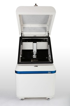
Park Systems Introduces the NX20 - Large Sample Atomic Force Microscope (AFM)


Park Systems introduces the NX20, a high-end, large sample atomic force microscope (AFM) for failure analysis (FA) and quality assurance (QA) laboratories that will benefit from the best available accuracy and reliability. 

The NX20 is the newest model of the NX product line with the world's most accurate AFM. Designed for the needs of FA and QA in the hard disk drive and semiconductor industries, the NX20 stands out for its unmatched non-contact mode that guarantees long-running probe tip sharpness. That's the key to the highest accuracy and repeatability for roughness measurement and defect review. It's also key to high productivity and the lowest AFM lifecycle costs.


"Our technology has been proven in the most demanding applications for nanoscale measurements in industry," said Dr. Sang-il Park, the founder and CEO of Park Systems. "NX20 builds on Park's long history of technology leadership in AFM accuracy and its reputation as the nanotechnology solutions partner to research and  industry. Our True Non-Contact Mode preserves the tip for much longer tip life and provides the most accurate measurements and images available for the most critical analysis requirements." 

The advantages of the NX20 for FA and QA highlight Park's True Non-Contact ModeTM where the probe tip reliably remains above the surface of the sample, thanks to the decoupled Z-dimension positioning servo with the fastest response time in the industry. With True Non-Contact ModeTM Park technology delivers non-contact AFM imaging without compromising measurement accuracy or user productivity. It also dramatically reduces tip replacement costs by extending tip lifetime. The NX20 also features True Sample TopographyTM, Park's unique technology for measuring the Z position with an industry-leading low noise Z-detector. This feature removes the effects of edge overshoot or piezo creep. Park AFM technology provides FA and QA labs with extremely accurate surface roughness measurements for media and substrates, defect review imaging and analysis, high resolution electrical scan mode and with decoupled XY scanning, sidewall measurments for 3D structure study.
"As critical dimensions shrink and device complexity increases, the quality of your data is critical for the success of your research, analysis, and ultimately device yield.  The key to quality results is accuracy at the nanoscale.  Accurate and repeatable measurements mean greater productivity, better analyses and better business results. With Park NX20's True Non-Contact Mode, AFM tips last 10 times longer saving time and money. Park NX20's True Sample TopographyTM enables accurate surface height recording of sample surface with its industry leading low noise Z detector," said Ryan Yoo, Vice President of Global Sales and Marketing. "Park understands the industry need for an advanced AFM with an affordable lifecycle cost that delivers the accuracy, productivity and reliability. This is how Park has become the AFM of choice in the hard disk and semiconductor industry."
With the introduction of the NX20, Park Systems launches an AFM built for the needs of FA and QA labs. The high-end, large sample design provides the accuracy and productivity demanded by manufacturing semiconductors and disk drives, while lowering life-cycle costs. It also addresses the future with the flexibility to add a multitude of available AFM modes, including advanced options and modes for FA and QA that are in development. Technical data and sample measurements are available on request. For more information please contact psc@parkAFM.com or visit www.parkAFM.com/nx.

domingo, 18 de noviembre de 2012

Innovative Technique to Control Electrical Conductivity of Graphene


Researchers at the Nanoelectronics Research Institute of the National Institute of Advanced Industrial Science and Technology (AIST), in joint work with a NIMS team headed by Dr. Kazuhito Tsukagoshi, a MANA Principal Investigator at the NIMS International Center for Materials Nanoarchitectonics, developed a novel technique for controlling the electrical conductivity of graphene.


A team headed by Dr. Shu Nakaharai, a Designated Intensive Researcher at the Collaboration Research Team Green Nanoelectronics Center (hereinafter, GNC; Leader: Naoki Yokoyama), Nanoelectronics Research Institute (Director: Seigo Kanemaru), National Institute of Advanced Industrial Science and Technology (hereinafter, AIST; President: Tamotsu Nomakuchi), and Dr. Shinichi Ogawa, an Invited Researcher at the Nanoelectronics Research Institute, AIST Innovation Center for Advanced Nanodevices (Director: Hiroyuki Akinaga), in joint research with a team headed by Dr. Kazuhito Tsukagoshi, a MANA Principal Investigator at the International Center for Materials Nanoarchitectonics (hereinafter, WPI-MANA; Director-General: Masakazu Aono), National Institute for Materials Science (hereinafter, NIMS; President: Sukekatsu Ushioda), developed a novel technique for controlling the electrical conductivity of graphene.
In the technique developed in this research, a helium ion beam is irradiated on graphene using a helium ion microscope to artificially introduce a low concentration of crystal defects, and it becomes possible to modulate the movement of electrons and holes in the graphene by applying a voltage to the gate electrode. Although this phenomenon of conduction control by introduction of crystal defects had been predicted theoretically, there were no examples in which on/off operation at room temperature was achieved experimentally. It is possible to introduce the technique developed in this work in the existing framework of production technology, including large area wafers.
Details of this technology were presented at the 2012 International Conference on Solid State Devices and Materials (SSDM2012) held in Kyoto, Japan September 25-27, 2012.

miércoles, 14 de noviembre de 2012

Peptides Self-Assemble into Nanofibers and Can Form Hydrogels


Smart scaffolding that can guide cells, proteins and small-molecule drugs to make new tissue and repair damage inside the body is in the works at Rice University.

Scientists at Rice and the Texas A&M Health Science Center Baylor College of Dentistry received a $1.7 million, five-year grantfrom the National Institutes of Health (NIH) to develop a hydrogel that can be injected into a patient to form an active biological scaffold.
Rice bioengineer Jeffrey Hartgerink and co-investigator Rena D'Souza of Baylor won the grant to continue their groundbreaking work on self-assembling, multidomain peptide hydrogels that not only physically support but alsoencourage the growth of specific kinds of tissues.
Bioengineers use scaffolds to mimic the body's extracellular matrix, which supports the growth and maintenance of living cells. Synthetic scaffolds are used as frameworks to form replacement tissues and, perhaps someday, regenerate entire organs from a patient's own cells. Once their work is done, the scaffolds are designed to degrade and leave only natural, healthy tissue behind.
While much of the work to date has focused on creatingtissue in the laboratory for implantation, Hartgerink's aim is to inject scaffolds infused with living cells that will allow the repairs to happen inside the tissue's natural environment.
The peptides designed and prepared at Rice self-assemble into nanofibers that can be triggered to form a hydrogel. "We can then deliver cells, small-molecule drugs and proteins to bring everything together properly in one place," said Hartgerink, an associate professor of chemistry and of bioengineering at Rice. Hydrogels could be designed to interact with stem cells and "get them to do what we want them to do," he said.
Hartgerink and D'Souza, a professor in the Department of Biomedical Sciences at Baylor currently on aworking sabbatical at Rice's BioScience Research Collaborative, have been pursuing the project for five years. The NIH grant will allow them to focus on the regeneration of the dentin-pulp complex found inside every tooth. The pulp, D'Souza said, is the soft tissue in the roots and crown that keeps the tooth vital and responsive to injury. "If you have a toothache, it's the tissue that's inflamed and has no place to expand. That's why it hurts so much," she said.
Currently, dentists remove inflamed pulp and replace it with an inert rubber-based filler, she said. But injecting stem cell-seeded hydrogels would allow natural pulp to regenerateinto the chamber while stimulating new dentin formation. "Hydrogels have key advantages," D'Souza said. "We can deliver them in a syringe to small spaces that are difficult to access, and the material does not get damaged. Developing this material as a restorative therapy is advantageous to patients as, unlike all other dental materials, this one is biologically active."
The researchers reached a milestone in 2010 when they found a way to have the fibers degrade rather than stay in the body. With the new grant, they hope to start trials of their dental hydrogel within two years, D'Souza said. "I can see potential applications for hydrogel, for example, for spinal cord regeneration or for various eye conditions, where we can restore the vitreous humour," she said.
Hartgerink is glad to have the NIH on board, but noted the grant would not have been possible without initial support from the Welch Foundation. "I've had Welch funding since the day I got here, and it has allowed me to do the preliminary work for all the grants we ended up getting," he said. "It's good to have them in Texas."
D'Souza said the seed grant money provided by the International Association for Dental Research in collaboration with GlaxoSmithKline enabled her laboratory to perform proof-of-concept stem cell experiments. "This is a great example of the huge benefits of interdisciplinary collaboration where, by combining expertise, we can push the frontiers of translational and clinical research forward."
Source: http://www.rice.edu/

viernes, 9 de noviembre de 2012

MIT Researchers Produce Electronic Components from Graphene-Like Molybdenum Disulfide


The discovery of graphene, a material just one atom thick and possessing exceptional strength and other novel properties, started an avalanche of research around its use for everything from electronics to optics to structural materials. But new research suggests that was just the beginning: A whole family of two-dimensional materials may open up even broader possibilities for applications that could change many aspects of modern life.

The latest “new” material, molybdenum disulfide (MoS2) — which has actually been used for decades, but not in its 2-D form — was first described just a year ago by researchers in Switzerland. But in that year, researchers at MIT — who struggled for several years to build electronic circuits out of graphene with very limited results (except for radio-frequency applications) — have already succeeded in making a variety of electronic components from MoS2. They say the material could help usher in radically new products, from whole walls that glow to clothing with embedded electronics to glasses with built-in display screens.
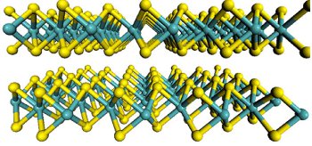
Diagram shows the flat-sheet structure of the material used by the MIT team, molybdenum disulfide. Molybdenum atoms are shown in teal, and sulfur atoms in yellow. Image courtesy of Wang et al.
A report on the production of complex electronic circuits from the new material was published online this month in the journal Nano Letters; the paper is authored by Han Wang and Lili Yu, graduate students in the Department of Electrical Engineering and Computer Science (EECS); Tomás Palacios, the Emmanuel E. Landsman Associate Professor of EECS; and others at MIT and elsewhere.
Palacios says he thinks graphene and MoS2 are just the beginning of a new realm of research on two-dimensional materials. “It’s the most exciting time for electronics in the last 20 or 30 years,” he says. “It’s opening up the door to a completely new domain of electronic materials and devices.”
Like graphene, itself a 2-D form of graphite, molybdenum disulfide has been used for many years as an industrial lubricant. But it had never been seen as a 2-D platform for electronic devices until last year, when scientists at the Swiss university EPFL produced a transistor on the material.
MIT researchers quickly swung into action: Yi-Hsien Lee, a postdoc in associate professor Jing Kong’s group in EECS, found a good way to make large sheets of the material using a chemical vapor deposition process. Lee came up with this method while working with Lain-Jong Li at Academia Sinica in Taiwan and improved it after coming to MIT. Palacios, Wang and Yu then set to producing building blocks of electronic circuits on the sheets made by Lee, as well as on MoS2 flakes produced by a mechanical method, which were used for the work described in the new paper.
Wang had been struggling to build circuits on graphene for his doctoral thesis research, but found it much easier to do with the new material. There was a “hefty bottleneck” to making progress with graphene, he explains, because that material lacks a bandgap — the key property that makes it possible to create transistors, the basic component of logic and memory circuits. While graphene needs to be modified in exacting ways in order to create a bandgap, MoS2 just naturally comes with one.
The lack of a bandgap, Wang explains, means that with a switch made of graphene, “you can turn it on, but you can’t turn it off. That means you can’t do digital logic.” So people have for years been searching for a material that shares some of graphene’s extraordinary properties, but also has this missing quality — as molybdenum disulfide does.
Because it already is widely produced as a lubricant, and thanks to ongoing work at MIT and other labs on making it into large sheets, scaling up production of the material for practical uses should be much easier than with other new materials, Wang and Palacios say.
Wang and Palacios were able to fabricate a variety of basic electronic devices on the material: an inverter, which switches an input voltage to its opposite; a NAND gate, a basic logic element that can be combined to carry out almost any kind of logic operation; a memory device, one of the key components of all computational devices; and a more complex circuit called a ring oscillator, made up of 12 interconnected transistors, which can produce a precisely tuned wave output.
Palacios says one potential application of the new material is large-screen displays such as television sets and computer monitors, where a separate transistor controls each pixel of the display. Because the material is just one molecule thick — unlike the highly purified silicon that is used for conventional transistors and must be millions of atoms thick — even a very large display would use only an infinitesimal quantity of the raw materials. This could potentially reduce cost and weight and improve energy efficiency.
In the future, it could also enable entirely new kinds of devices. The material could be used, in combination with other 2-D materials, to make light-emitting devices. Instead of producing a point source of light from one bulb, an entire wall could be made to glow, producing softer, less glaring light. Similarly, the antenna and other circuitry of a cellphone might be woven into fabric, providing a much more sensitive antenna that needs less power and could be incorporated into clothing, Palacios says.
The material is so thin that it’s completely transparent, and it can be deposited on virtually any other material. For example, MoS2 could be applied to glass, producing displays built into a pair of eyeglasses or the window of a house or office.
In addition to Palacios, Kong, Wang, Yu and Lee, the work was carried out by graduate student Allen Hsu and MIT affiliate Yumeng Shi, with U.S. Army Research Laboratory researchers Matthew Chin and Madan Dubey, and Lain-Jong Li of Academia Sinica in Taiwan. The work was funded by the U.S. Office of Naval Research, the Microelectronics Advanced Research Corporation Focus Center for Materials, the National Science Foundation and the Army Research Laboratory.
Source: MIT

viernes, 2 de noviembre de 2012

Solar Panels Kept Clean by Hydrophobic Nanoparticle Layer


A University of Houston researcher has developed a nanoparticle coating for solar panels that makes it easier to keep the panels clean, which helps maintain their efficiency and reduces the maintenance and operations costs.

The patent-pending coating developed by physics professor Seamus "Shay" Curran, director of UH’s Institute for NanoEnergy, has successfully undergone testing at the Dublin Institute for Technology and will undergo field trials being conducted by an engineering firm in North Carolina.
Curran said the June testing in Ireland and the field trials being done at Livingston & Haven in Charlotte, N.C., represent significant steps forward in moving the coating and a related technology to the marketplace. A demonstration of the coating was conducted Friday (Aug. 10) at Livingston & Haven.
The Self-Cleaning Nano Hydrophobic (SCNH107TM) layer has been licensed by C-Voltaics from UH. C-Voltaics, a start-up energy company dedicated to the generation of more practical clean energy for use in off-grid and on-grid applications, will oversee marketing of the coating and a "Storm Cell" - a transportable energy generator with unique patent-pending designs and engineering aspects that was also developed by Curran at UH.
Solar panels need to have a clean surface to efficiently gather light from the sun, but they are often soiled by dust, pollen, water and other particles. Curran’s coating acts as a barrier protection against these pollutants.
The nano-thin coating repels dust, pollen, water and other particles without hindering the solar panel’s ability to absorb sunlight. The coating can maintain this ideal hydrophobic surface for years, reducing overall maintenance.
"A dirty solar panel can reduce its power capabilities by up to 30 percent," Curran said. "The coating essentially makes the panel self-cleaning."
While the coating is designed for use on solar panels, Curran believes it could also have widespread applications as an anti-corrosive coating for other materials.
UH is a shareholder in C-Voltaics, which focuses on using technology to alleviate the significant costs of solar energy service and maintenance, which are key issues in solar energy generation and storage.
"This is where you see the university transitioning a technology from the lab to the community and making an economic impact," Curran said.
Curran developed the coating in conjunction with his work on building transportable, off-grid solar-powered generator for residential and commercial use.
Curran’s development of the storm cell system stems from his family’s experience during Hurricane Ike in September 2008. Curran, his wife and three young sons stocked up and hunkered down as Ike approached the Texas coast. They woke up the next morning after the storm passed with the house intact, but powerless.
"My wife said to me, ‘How long have you been working in solar energy? The sun is shining but we don’t have any electricity. Why don’t you build us a portable solar unit for the next time this happens?’"
The dutiful husband did as he was asked.
The solar-powered Storm Cell is designed to be used much in the same way as a diesel generator, except it’s quiet and has no emissions. It consists of a square storage trailer with solar panels attached to retractable arms that can be manually unfurled as needed and then stored inside the trailer.
The unit built by Curran and his team produces two-to-five kilowatts and charges a backup battery. That’s enough power for an air-conditioning system, some light and a TV. But Livingston & Haven has built an even larger unit that could fully power a 3,000-square-foot house. Curran said there also are a number of commercial uses for the generators such as oil and gas drill sites and farms.
The generator system will be engineered and sold by C-Voltaics and Livingston & Haven.
Curran has been involved in solar energy research for many years and also has been working on improving the efficiency of thin-film solar cells in terms of storing solar energy. Thin-film solar cells are lightweight, durable and easy to use. Researchers are trying to improve their efficiency in terms of storage capability so that they are competitive with silicon cells.
Curran also has created several innovations that relate to the next generation of solar devices used to produce electricity. These devices are all plastic, as opposed to the current devices that use silicon or metal alloys, which take up space and can be costly.

http://www.youtube.com/watch?feature=player_embedded&v=t-POIkdh_I8

miércoles, 24 de octubre de 2012

MIT Researchers Produce Electronic Components from Graphene-Like Molybdenum Disulfide


The discovery of graphene, a material just one atom thick and possessing exceptional strength and other novel properties, started an avalanche of research around its use for everything from electronics to optics to structural materials. But new research suggests that was just the beginning: A whole family of two-dimensional materials may open up even broader possibilities for applications that could change many aspects of modern life.

The latest “new” material, molybdenum disulfide (MoS2) — which has actually been used for decades, but not in its 2-D form — was first described just a year ago by researchers in Switzerland. But in that year, researchers at MIT — who struggled for several years to build electronic circuits out of graphene with very limited results (except for radio-frequency applications) — have already succeeded in making a variety of electronic components from MoS2. They say the material could help usher in radically new products, from whole walls that glow to clothing with embedded electronics to glasses with built-in display screens.
Diagram shows the flat-sheet structure of the material used by the MIT team, molybdenum disulfide. Molybdenum atoms are shown in teal, and sulfur atoms in yellow. Image courtesy of Wang et al.
A report on the production of complex electronic circuits from the new material was published online this month in the journal Nano Letters; the paper is authored by Han Wang and Lili Yu, graduate students in the Department of Electrical Engineering and Computer Science (EECS); Tomás Palacios, the Emmanuel E. Landsman Associate Professor of EECS; and others at MIT and elsewhere.
Palacios says he thinks graphene and MoS2 are just the beginning of a new realm of research on two-dimensional materials. “It’s the most exciting time for electronics in the last 20 or 30 years,” he says. “It’s opening up the door to a completely new domain of electronic materials and devices.”
Like graphene, itself a 2-D form of graphite, molybdenum disulfide has been used for many years as an industrial lubricant. But it had never been seen as a 2-D platform for electronic devices until last year, when scientists at the Swiss university EPFL produced a transistor on the material.
MIT researchers quickly swung into action: Yi-Hsien Lee, a postdoc in associate professor Jing Kong’s group in EECS, found a good way to make large sheets of the material using a chemical vapor deposition process. Lee came up with this method while working with Lain-Jong Li at Academia Sinica in Taiwan and improved it after coming to MIT. Palacios, Wang and Yu then set to producing building blocks of electronic circuits on the sheets made by Lee, as well as on MoS2 flakes produced by a mechanical method, which were used for the work described in the new paper.
Wang had been struggling to build circuits on graphene for his doctoral thesis research, but found it much easier to do with the new material. There was a “hefty bottleneck” to making progress with graphene, he explains, because that material lacks a bandgap — the key property that makes it possible to create transistors, the basic component of logic and memory circuits. While graphene needs to be modified in exacting ways in order to create a bandgap, MoS2 just naturally comes with one.
The lack of a bandgap, Wang explains, means that with a switch made of graphene, “you can turn it on, but you can’t turn it off. That means you can’t do digital logic.” So people have for years been searching for a material that shares some of graphene’s extraordinary properties, but also has this missing quality — as molybdenum disulfide does.
Because it already is widely produced as a lubricant, and thanks to ongoing work at MIT and other labs on making it into large sheets, scaling up production of the material for practical uses should be much easier than with other new materials, Wang and Palacios say.
Wang and Palacios were able to fabricate a variety of basic electronic devices on the material: an inverter, which switches an input voltage to its opposite; a NAND gate, a basic logic element that can be combined to carry out almost any kind of logic operation; a memory device, one of the key components of all computational devices; and a more complex circuit called a ring oscillator, made up of 12 interconnected transistors, which can produce a precisely tuned wave output.
Palacios says one potential application of the new material is large-screen displays such as television sets and computer monitors, where a separate transistor controls each pixel of the display. Because the material is just one molecule thick — unlike the highly purified silicon that is used for conventional transistors and must be millions of atoms thick — even a very large display would use only an infinitesimal quantity of the raw materials. This could potentially reduce cost and weight and improve energy efficiency.
In the future, it could also enable entirely new kinds of devices. The material could be used, in combination with other 2-D materials, to make light-emitting devices. Instead of producing a point source of light from one bulb, an entire wall could be made to glow, producing softer, less glaring light. Similarly, the antenna and other circuitry of a cellphone might be woven into fabric, providing a much more sensitive antenna that needs less power and could be incorporated into clothing, Palacios says.
The material is so thin that it’s completely transparent, and it can be deposited on virtually any other material. For example, MoS2 could be applied to glass, producing displays built into a pair of eyeglasses or the window of a house or office.
In addition to Palacios, Kong, Wang, Yu and Lee, the work was carried out by graduate student Allen Hsu and MIT affiliate Yumeng Shi, with U.S. Army Research Laboratory researchers Matthew Chin and Madan Dubey, and Lain-Jong Li of Academia Sinica in Taiwan. The work was funded by the U.S. Office of Naval Research, the Microelectronics Advanced Research Corporation Focus Center for Materials, the National Science Foundation and the Army Research Laboratory.
Source: MIT

viernes, 5 de octubre de 2012

Nanotechnology in Aerospace Materials


Figure 1. The aerospace industry is under pressure to improve it's environmental footprint, primarily by making aircraft more efficient. 
The aerospace industry is one of the most important heavy industries in the world. Countless companies rely on the ability to ship products and people around the world with the speed that can only by achieved by air. The aircraft manufacturing market was worth xxx billion in 20xx, and the bulk of this was accounted for by military spending.
Along with this huge economic value, however, comes huge consumption, and one of the largest carbon footprints on the planet relative to the size of the market. For this reason, the major drivers in current aerospace R&D are towards lighter construction materials and more efficient engines - the overall goal being to reduce fuel consumption and carbon emissions associated with air travel and air freight. The significant interest in nanotechnology for the aerospace industry is justified by the potential of nanomaterials and nanoengineering to help the industry achieve this goal.
This article will review some of the nanomaterials which are already being applied in aerospace manufacturing, and the benefits they can provide.

Nanostructured Metals

Bulk metals with some nanoscale structure are already widely used in aircraft manufacturing. It is now well known that nanostructured metals - exhibit considerably improved properties compared to their counterparts with microscale or larger grain structure.
This is particularly noticeable for properties which are crucial for materials used in aircraft - primarily yield strength, tensile strength and corrosion resistance, coupled with low density which helps keep the total weight of the aircraft down.
Figure 2. Bulk nanostructured metals exhibit much better mechanical properties and corrosion resistance than their counterparts with larger crystal structures.

Polymer Nanocomposites

Various nanomaterials have been used as filler materials to enhance the properties of structural and non-structural polymers used in aircraft construction. The most commonly used nanomaterials include nanoclays, carbon nanotubes, nanofibres, and graphene.
Carbon nanotubes in particular have been shown to give excellent advantages when used as fillers in various polymers, due to their exceptional stiffness, toughness, and unique electrical properties.
Nanocomposites typically have superb weight-to-strength ratios, and enhanced resilience to vibration and fire, making them ideal for use in the aviation industry. The properties of the nanofillers, like the conductivity of nanotubes, for example, can create interesting opportunities for multifunctional materials.
The properties of polymers enhanced by nanomaterial fillers are so well-tuned to the requirements of aircraft manufacturers, that they are actually being used to replace some of the metals used in the airframes. This obviously brings along huge weight savings, and often cost savings as well.

Tribological and Anti-Corrosion Coatings

Another major trend in the materials used in aircraft is towards nanocoatings to enhance the durability of metals. In particular, magnesium alloys, which are far lighter than steel or aluminium, are prone to corrosion, due to the high chemical reactivity of magnesium. Coatings can help prevent corrosion, but the type typically used contain chromium complexes which are a highly toxic pollutant.
Materials used for these novel anti-corrosion nanocoatings include silicon and boron oxides, and cobalt-phosphorous nanocrystals.
Nanocoatings are also now being used on turbine blades and other mechanical components which have to withstand high temperatures and friction wear. Tribological coatings can drastically lower the friction coefficient and improve resistance to wear - this greatly improves the efficiency of the engines.
Many nanostructured and nanoscale coating materials have been suggested as possible friction modifying agents, such as carbides, nitrides, metals, and various ceramics.
Figure 3. The defense sector drives a lot of the innovation in many industries, and aerospace is no exception. High-performance military aircraft require exceptional materials, which will eventually find their way into commercial vehicles. 


This is just a brief overview of some of the nanomaterials being used in aerospace. The drive for lighter and more efficient air vehicles has led to the rapid adoption of nanotechnology in aerospace manufacturing.
The main roadblock, as with many industries looking to adopt nanotechnology, is caused by uncertainty over the environmental and health and safety implications of these materials. Whilst nanomaterials can often be less toxic than the current materials used, the effects of long-term exposure to these novel materials are still uncertain.
The potential of nanotechnology in the aerospace industry cannot be denied, however. Outside of airframe and component materials, nanotechnology applications have been found in lubricants, fuel, adhesives and many other areas.
Nanotechnology is also helping engineers to create vehicles with the necessary properties to endure the harsh conditions of space.

domingo, 30 de septiembre de 2012

New Technique to Fabricate Semiconductors from Graphene


Dr. Helge Weman and Professor Bjørn-Ove Fimland, researchers from the Norwegian University of Science and Technology (NTNU), have become the first in the world to devise a technique for semiconductor production from graphene.


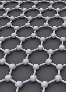
Graphene comprises a single layer of carbon atoms. (illustration: Wikimedia Commons).

In this technique, a network of semiconductor nanowires is grown on graphene by bombarding its surface with arsenic molecules and gallium atoms. The resulting product is a 1-µm thick hybrid material that behaves as a semiconductor. By contrast, existing silicon semiconductors have several hundred folds thickness and their electrical conductivity gets affected by light, temperature or the inclusion of other atoms.
According to Weman, the ability to fabricate graphene-based semiconductors opens the door to produce more efficient and inexpensive semiconductor components when compared to existing silicon-based components. A material with a flexible and transparent base may transform the production of LED components and solar cells. Conventional windows in houses may also serve as television screens and solar panels. It may be possible to use mobile phone screens as a wrist watch.
Research Council’s Clean Energy for the Future Programme funded the basic research that led to these breakthrough findings, while Nanotechnology and New Materials program that concluded recently had initiated the findings.
The researchers have obtained support in securing patents and establishing a company from NTNU Technology Transfer, a joint partner to the program titled ‘Commercialising R&D Results (FORNY2020) at the Research Council of Norway.’ They will now start the production of prototypes for specific applications. Electronic giants like IBM and Samsung have been in touch with the researchers.
The research team believes that the new semiconductor hybrid materials will be commercially available within five years.
Source: http://www.forskningsradet.no

lunes, 24 de septiembre de 2012

New Stamping Process to Produce Precise Biomolecular Structures at Nanoscale


Making accurate biomolecular structures at small scales is significant to the advancement of nanotechnology and other related fields. Traditionally, this has been accomplished by using rubber stamps with small features that are enclosed with molecular "inks" and later stamping onto substrate surfaces to produce a molecular pattern. However, molecules tend to disperse on the surface during and after the process of stamping and blur the patterns.


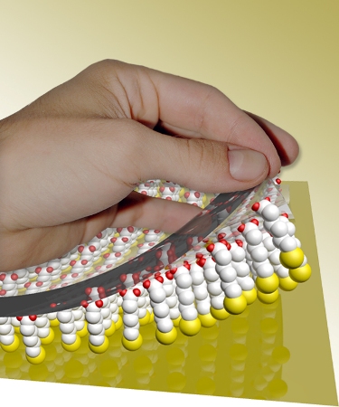
Reactive stamps remove molecules from surfaces to create precise nanoscale patterns.

Researchers from UCLA have reversed this traditional "soft lithography" process in order to address this problem. They utilized stamps that were chemically treated, instead of utilizing a stamp to shift molecules to bare surfaces, to remove molecules placed already on gold substrates and peel away specific molecules through chemical bonds in order to create accurate patterns.
The new process, dubbed chemical lift-off lithography (CLL), eliminates the blurring problems found in earlier techniques and achieves higher-resolution patterning. The research findings are published in the journal Science.
The stamp, utilized in the new process, is designed by using a “master” shaped with expensive and sophisticated tools; it can be used regularly. An oxygen plasma reactivates stamps between each use. The chemical bonds created at the stamp-substrate interface remove boththe molecules in the monolayers as well as the sheet of gold atoms from the substance. The researchers found that monolayers and gold–gold bonds break easily compared to molecule–gold bonds.
During the research, different types of high-resolution patterned features were fabricated, and stamps were refined and reused over and over again with minimum feature deterioration. The research team also found that the remaining monolayer can resist etching exposed gold features. New molecules backfilling into the lifted-off areas allowed patterned protein capture and precise 40 nm chemical patterns were attained.
When individual masters are created, CLL is utilized for high-throughput, high-resolution pattern fabrication. This procedure allows patterns to be moved to substrates, and various stamping strategies can be utilized to produce nanometer-scale patterns with high fidelity on gold substrates.
Source: http://www.ucla.edu/

jueves, 30 de agosto de 2012

Researchers Discover Self-Healing Property of Graphene


By Will Soutter

A team of researchers from the SuperSTEM facility at Science & Technology Facilities Council’s Daresbury Laboratory and The University of Manchester has found that graphene, a one-atom-thick carbon material, undergoes a self-mending process to repair holes.


SuperSTEM2, there are only six of these exceptionally sensitive instruments worldwide (credit: SuperSTEM Consortium))

This finding is a significant breakthrough to realize the nanomaterial’s vast potential in a myriad of applications ranging from medicine to electronics. The study is reported in the journal, Nano Letters.
The research team, which consisted of Nobel Prize-winner Professor Kostya Novoselov, was actually exploring the mechanism behind the interaction of metal with graphene, which is important for the integration of nanomaterial into future electronic devices.
For the study, the research team used a powerful electron microscope at the SuperSTEM Laboratory that enables researchers to explore material properties one atom at a time. The team recently showed that metals are capable of initiating the creation of holes in a graphene sheet. This may affect the characteristics of any graphene-based device.
However, what surprised the research team was some of the holes formed in this process were re-knitting the graphene structure by self-mending spontaneously utilizing adjacent loose carbon atoms.
SuperSTEM’s Scientific Director, Dr Quentin Ramasse stated that the fact that graphene is capable of self-healing under the right conditions could differ a proof of concept and a working device without any practical application. Now, there is a method that allows the drilling of the nanomaterial in a controlled manner to shape it at the atomic level and to grow it back in novel shapes. This provides more options to the nanotechnology toolbox, thus opening the door to future technological applications.
Source: http://www.stfc.ac.uk

martes, 28 de agosto de 2012

New Non-Invasive Microscopy Tool to Analyze Nanostructures


By Will Soutter

Scientists at the University of Sheffield have created a radical analytical tool that can be used to study nanometer scale devices without damaging them. The device which adopts nuclear magnetic resonance technique will enable further advancement in nanotechnology by facilitating researchers to gain better insight into nanostructures.


Image of Nanostructures (©iStockphoto.com/shunyufan)

Before the development of this innovative tool by the Department of Physics and Astronomy in University of Sheffield, researchers have had to deal with the limitation of existing study techniques in which the materials are irrevocably damaged. New nanoscale materials can be developed only if there is an understanding of the formation process of existing nanostructures and their properties. When the nanostructures are damaged during experimentation, the information on the vital link between the structural and photonic or electronic characteristics of the material is unobtainable.
The new non-invasive nuclear magnetic resonance (NMR) probing opens up new vistas for nanoengineering by enabling complete characterization of new materials and subsequently paving the way for new device fabrication techniques.
Research team lead, Dr Alexander Tartakovskii stated that the focus of their research was semiconductor quantum dots for their potential photonic applications and future quantum computer applications. Through the study, his team was able to gain more insight into the chemical composition of quantum dots and the difference in atomic alignment within the quantum dots vis-à-vis perfect crystals. The quantum dots remained intact for further magnetic and optical property measurements even after the NMR probing.
Source: http://www.shef.ac.uk/